How to Design a Smartwatch PCB Assembly Solution?
In the context of rapid iteration in wearable devices, smartwatch PCB assembly (PCBA) not only faces stringent space constraints but also requires finding the optimal balance between high integration and long battery life.
As consumers become increasingly reliant on functions such as health monitoring, GPS positioning, and Bluetooth calling, the complexity of motherboard design is increasing exponentially.

I. Defining Core Design Requirements and Space Planning
Size and Thickness Limitations: The internal space of smartwatches is extremely limited. PCBs typically require irregular shapes (such as circular or racetrack-shaped), and the thickness must be controlled to below 0.6mm.
Multilayer Boards and HDI Processes: To accommodate high-density chips, high-density interconnect (HDI) technology must be used. This involves arbitrary layer interconnects or stepped laser drilling to achieve the routing of micro BGAs and fine-pitch components.
Rigid-Flex PCB Applications: By rationally planning rigid and flexible areas, the battery, display, sensors, and buttons can be seamlessly connected via FPC, significantly reducing the space occupied by traditional connectors.
II. Component Selection and Layout Optimization
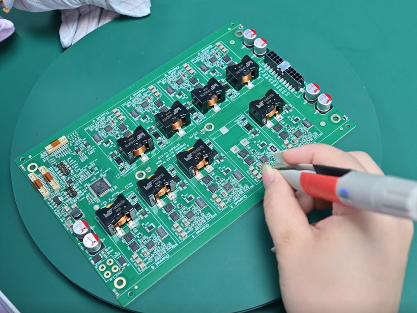
Main Control Chip and Power Management (PMIC): Prioritize highly integrated SiP (System-in-Package) modules, integrating the main processor, memory, and RF unit into a single unit to shorten signal paths and reduce the number of discrete components.
Thermal Design and Power Consumption Balance: To address the heat generated by the processor under high load, the layout must keep heat sources away from the screen and skin contact surfaces, and reserve space for heat dissipation copper foil or thermally conductive sealant in critical areas.
RF and Sensor Interference Immunity: Heart rate sensors (PPG), gyroscopes, and Bluetooth/GPS antennas are highly susceptible to electromagnetic interference. The layout must strictly adhere to high-frequency signal isolation principles, and a shielding can must be installed at the RF front end.
III. Manufacturing Process and SMT Assembly Control
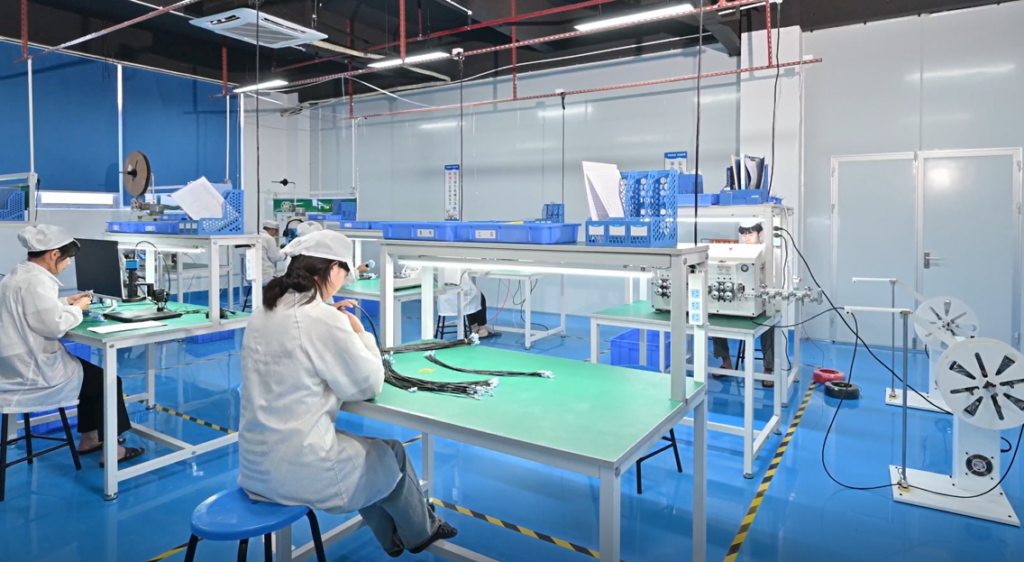
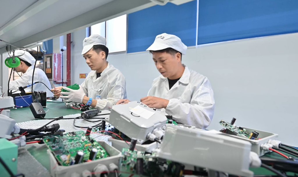
Fine-Pitch Placement Accuracy: For resistors and capacitors with dimensions of 0201 or even 01005 and fine-pitch QFN/BGA packages, the SMT production line must be equipped with high-precision placement machines and 3D SPI (solder paste inspection) to ensure accurate solder application.
Precision Soldering and Underfill: Due to the frequent shocks and drops during daily wear, BGA and core chip assembly requires underfill adhesive to enhance resistance to drops and mechanical stress.
Proof Coating and Waterproof Coating: To address potential exposure to sweat, rain, or swimming, the PCBA surface must be uniformly coated with a nano-waterproof coating or locally sealed with adhesive to ensure IP68 water resistance.
IV. Testing and Quality Verification System
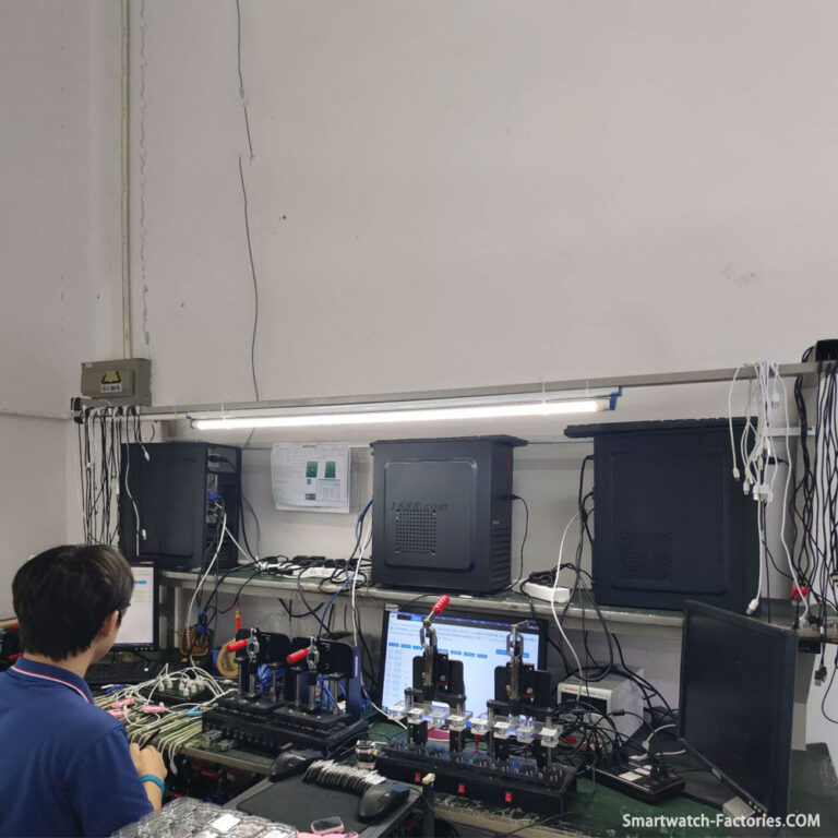
In-Circuit Testing (ICT) and Functional Testing (FPT): Rigorous electrical performance testing is conducted after assembly to verify the response speed and RF transmission power of each sensor.
High and Low Temperature Testing and Reliability Aging: Simulating extreme usage environments, PCB components undergo thermal shock, drop testing, and micro-motion fatigue testing to ensure high yield rates for large-scale mass production of smartwatches from the outset.
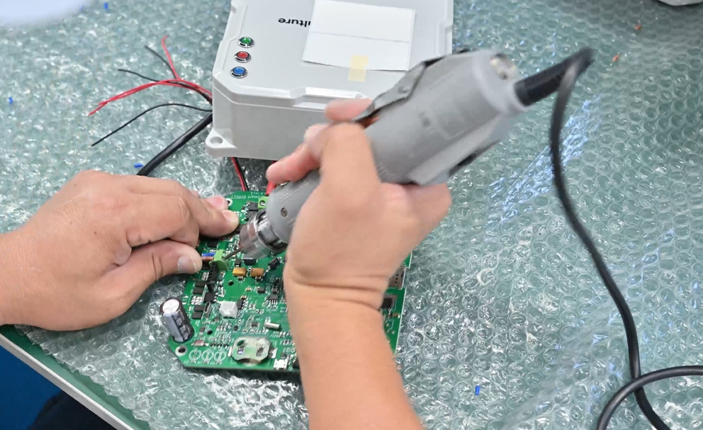
At a leading PCB manufacturing and assembly plant in China, leveraging our global high-end supply chain advantages, we focus on providing highly reliable end-to-end PCB manufacturing and assembly services.
As a leading provider of rapid circuit board manufacturing, multilayer board production, PCBA electronic component placement, SMT manufacturing, and DIP insertion solutions, we deeply empower global electronic innovation with cutting-edge intelligent manufacturing processes and superior quality.